Major Subsystems: Hardware, Firmware, System Software, and Applications.
A complete instrument is composed of several major parts and subsystems, here listed bottom-up. The hardware comprises the lowest layer. The top layer is the application software which provides the look-and-feel of the instrument. The firmware is in the middle. From the software standpoint the firmware is very much the same as the real hardware, because both the physical hardware and the firmware are composed of logic elements, whose place of residence is secondary. For the software it does not matter whether a given piece was soldered to the board (hardware), or declared in the HDL (firmware). The following layers comprise the computerized instrument.
- The hardware board with all the needed components, interfaces, and periherals: the FPGA, RAM, SD card, communication, analog converters, etc.
- The Oberon System On Chip (SOC) comprising the soft processor core, the memory bus, and firmware interfaces for the standard peripherals: RAM, SD card, mouse, keyboard, etc. The SoC firmware is functionally pretty much the same for both Astrobe and the full Oberon System.
- The Application Firmware, comprising firmware interfaces for analog converters and other application hardware, which were not present in the original 2013 FPGA Oberon SoC.
- The core Oberon System software drivers for all the standard firmware and hardware pieces provided with the original SoC: mouse, keyboard, SD card, serial link, etc. This layer is functionally pretty much the same for both Astrobe and the full Oberon System.
- The upper layer of the FPGA Oberon System: the editor, compiler, and graphical viewer management.This layer is present in the full Oberon System and absent in Astrobe. In the latter case it was factored out and moved to the host computer. Please read the overview of the Astrobe development system for details.
- The General Application Software, enhancing the functionality of the instrument. Several major applications can be ported from Linz Oberon V4 to the FPGA Oberon System. Graphical editor Kepler, network utilities, enhanced wordprocessor with active elements, compiler tools, a lean Dialogs GUI, and many other useful applications are offered by V4. Another rich repository of such applications is ETH System 3, which however needs more RAM and uses more CPU power.
- The Specific Application Software, providing the specific functionality of the instrument. The B2 Data Analysis Framework will become a basis for developing the table top Nuclear Physics data acquisition running under the full Oberon System. In case of Astrobe, a similar (albeit less comprehensive) function can be implemented with a small TFT display shown on the Astrobe page. Such a display would be appropriate for a portable hand-held data acquisition instrument.
The bits and pieces listed above do not need to be developed in sequence. The major development steps can proceed in parallel thanks to a rich repertoire of available development tools. For example, Oberon system software can be worked out under a RISC5 emulator running on a regular PC. B2 development can be continued under the Linz V4 environment, hosted under Windows or Linux. Customizing B2 to the needs of the table top DAQ can be completed under an emulator without accessing physical ADC hardware. In the past I developed the Gr Data Acquisition and Monitoring Toolbox for BlackBox, using this approach. (Click on the preceeding link, and scroll down to Gr.)
Development Priorities: Hardware, Firmware, System Software, or Applications?
Two years ago I was thinking that hardware had to be developed first, followed by firmware, system software, and finally some cool applications. In other words, I followed a bottom up approach. But now I think that a more efficient path will focus on the software, taking advantage of available emulators. Using an emulator we can refine the system drivers, display, user interface, as well as the graphical B2 framework which will be used in research instruments.
An important prerequisite for efficiently using the emulators is that the board(s) and the emulators remain in synch. It can be realized if the future firmware keeps all the original peripheral addresses intact, because these are hardwired into the emulators. Later on we will hopefully learn how to modify the emulators, or at least one of them. (Michael's emulator, because it supports a color display.) We will then be in the position to release the hardware board, its firmware, and a modified emulator accurately representing the instrument. Until this happens we will simply stick to the original addresses in firmware.
The Most Recent RiskFive Firmware.
The most recent RiskFive firmware was developed by Vedant Karia under Vivado 2018.3 (64-bit). It is available from the following link (file size 7,337 kB). Despite the name "final" it is far from being finished. There are still some subtle timing issues which we did not resolve before Vedant left. The original Oberon System software could boot under this firmware, but then we could not make the mouse and the keyboard to work. A few months later I discovered that the mouse and keyboard register addresses were swapped in Input.Mod at the software side of the Oberon System. This is where the work has stopped at the moment.
Critical assessment of the original FPGA Oberon design.
Before outlining the detailed plan we need to thoroughly asses the overall situation with the FPGA Oberon. It was originally developed as a one-off effort preserving the original 1992 Ceres Oberon System architecture within limited resources of the Spartan-3 Starter Kit. Despite its frugal design, the SoC firmware filled 95.4% of the FPGA, leaving no space for any extra firmware components. The design did not provide for a firmware extension framework such as Wishbone, because there was no space to add any extensions anyway. A few essential peripherals were mapped through registers spaced four address locations (16 bytes) apart.
The following peripherals were mapped in the original Oberon SoC at the high CPU memory addresses (FFFFFFxx in hex notation): a millisecond counter, switches and LEDs, serial RS-232, SPI, PS2 keyboard, and PS2 mouse. There were no explicit provisions for adding extra peripherals. It was implied that the adopted addressing scheme will be either applied as is, or somehow modifed while adding new peripherals, but the specification was not provided. The original addressing scheme will be fairly restrictive when adding complex peripherals with larger numbers of control registers.
Oberon SoC coding style is compounding the problem. The register addresses were not factored out into a separate file or a Board Support Package (BSP), as it is customary in the FPGA industry. They were rather hardwired directly into the top level HDL file in a very peculiar fashion. For example, the memory address of the system counter (address FFFFFFC0) was decomposed in Verilog into 03FFFF plus separate lower bits, because the most significant address bits were not routed outside the CPU. There were no comments in the Verilog code explaining the reason for writing 03 rather than FF for the most significant bits.
To further compound the problem, the same address was accessed as "-64" in the software, because Oberon language lacks support for unsigned 32-bit integers. It only supports the signed integers, where the highest bits "FF..." represent a negative signed number. This kind of coding discrepancies would have been less confusing if they were thoroughly documented in the code, which however was not the case.
We are also facing two more related problems. Fortunately, they can be circumvented, as I will describe below.
- First, the system addresses mentioned above were not factored into a single "include" file in the software part of the system. They were rather repeated verbatim wherever they were used in the code. The proliferation of verbatim numbers will make a modification of the addressing scheme a tedious task.
- Second, the same addresses were also hardwired into the emulators. This is probably the biggest problem of all. Changing the addressing scheme at the board level will break the connection between the board and the emulators, rendering the emulators less useful. It would be very inconvenient.
So now we need to overcome these limitations if we want to develop useful applications running on more powerful FPGAs, larger memories, additional peripherals, and better graphics. A brute force approach would consist of fixing the source code in all relevant places: the SoC firmware code, the software drivers, and the emulators. It can be done, but the problem will return with every fresh release of the tools by other developers who do not deem such modifications desireable to pursue their own goals. So we need to figure out a more conservative development path.
Development Goals and Steps.
We want to achieve the following goals, while fullfilling the constraints.
- Goal. Restructure the SoC to aid future maintainance and modifications. Reformat the code to decrease the hostility. Adding comments will help a lot even without actual changes. Since we plan extensive changes anyway, we do not need to treat the SoC code like a gospel. We can change it quite extensively, subject to the constraints.
- Goal. Provide a mechanism for adding additional peripherals to the board, such as ADCs, the Ethernet chip, WiFi, etc.
- Goal. Document the addressing and other similar peculiarities mentioned above. Add comments to both the SoC firmware and to the low level software. Alternatively and in parallel, develop the documentation separate from the software modules to avoid the situation, that the 3rd party developers keep releasing undocumented code. (They have done it in the past.)
- Constraint. Do not break the connections with the higher level software. Keep the interfaces intact between the modified low level drivers and the mid level modules. Be prepared for the situation that the 3rd party developers release their updated tools planted on the original drivers. (They have done it in the past.)
- Constraint. Do not break the connections between the firmware and the emulators. Since it is virtually guaranteed that the emulators will not change, it means that all the original peripherals must keep their current memory addresses in the SoC.
- Goal. Develop the method to write FPGA configuration into the FPGA flash chip. This is a workaround for Xilinx's lack of support for certain flash chips. When I designed RiskFive, it never occured to me that Xilinx will not support the most common Winbond flash. We will need to develop a method to save the configuration file into that flash, bypassing the Xilinx toolchain.
- Goal. Develop the RISC5 Microcontroller System (RCS) in analogy to the MicroBlaze Microcontroller System (MCS) described in the SoC textbooks by Pong P. Chu. The RCS will internally provide all the original peripherals at the original addresses. It will preserve the compatibility with the emulators.
- Goal. Provide a robust memory bus outside the RCS. The choices include the present SoC bus (yes, there is one already), the FPRO bus by Pong P. Chu, Wishbone, or some other design. Avoid AXI by Xilinx, because it is proprietary. Our planned applications do not call for this level of complexity.
- Goal. Provide the ZBT memory controller and interface it to the memory bus. The first draft is available in the RiskFive firmware linked earlier on this page.
- Goal. Since we will provide more memory (4 MB) than the original SoC (1 MB), we also have to change the memory map of the software system. This has to be done very thoroughly and with detailed documentation, because we will need to move the heap, the stack origin, etc. The problem is not so much how to do it, but rather how to convince the 3rd party developers to stop coming back with the old values. Ideally we can convince them to parametrize their software to support various memory sizes and maps. This work can be completed under the emulator.
- Goal. Provide color graphics. Initially 4-bit (16 colors) which has already been done by Magnus and Joerg. Down the road we are aiming at 8-bit (256 colors) using 1 megabyte of RAM for a frame buffer. The software interface to the color display can be completed under the emulator.
- Goal. Port Linz V4 to the FPGA Oberon. This can be done under Michael's emulator running the Extended Oberon System by Andreas. We do not need the physical board to do it.
- Goal. Develop the Ethernet interface using either W5500, W5300, or both. If both, then the interface needs to be parametrized to provide a uniform software driver. Do not use the SGMII provided with RiskFive prototypes because it is unlikely to work with the silicon grade on these boards.
- Goal. Develop the Ethernet communication using the chip(s) listed above.
- Goal. Port the Internet utilities from Linz V4 or ETH System 3 to FPGA Oberon, using the above as the physical interface. Part of this work can be done under an emulator. Michael expressed some desire to provide an emulated Ethernet chip.
- Low priority goal. Develop the dual-port access to the ZBT buffer to completely decouple the CPU from the screen refresh. Note that a large HyperRAM frame buffer is preferred over the ZBT frame buffer, but using HyperRAM will require a new board design.
- Future design goal. Provide a much larger RAM. Use HyperRAM because the board layout will be reasonably easy. This memory may work even without cache at some performance loss. In a long run we will need to add the cache. Cache has already been implemented by Magnus and Joerg.
- Future design goal. Provide a large screen. Use HyperRAM for a frame buffer. Example: 1920 x 1200 pixels at 16 bit color will take 4,608,000 bytes. This will fit into a single 8 MB HyperRAM chip. This is a long term project requiring a new board with HyperRAM in addition to ZBT.
- Future design goal. Provide variable screen size. Ideally the firmware will be able to query the HDMI monitor, but this may be an overkill. Being able to change the screen manually will be good enough. It may lead to messed up display. Provide a recovery mechanism, such as rolling back to a good known setup upon pressing a dedicated push button.
- Low priority goal. Reformat and document the HDL code of the RISC5 soft core to aid understanding how it operates. It is not strictly necessary, but better understanding of the code will help in the long run. It is also possible that we will need to dig into the floating point implementation which was recently discussed in the mailing list. Constraint. Do not modify the CPU instructions.
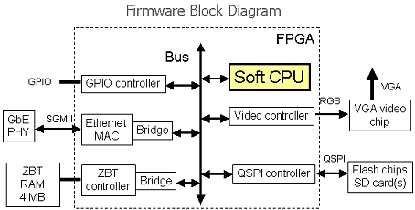
Figure 1. Conceptual block diagram of the firmware. The SGMII interface is unlikely to work with RiskFive protypes because of the speed grade of the soldered Artix-7.
Hardware development tools.
- Power supply +5V with the OD = 5 mm, ID = 2.1 mm barrel connector. Recommended power supplies from Jameco with 2.1 mm connectors: Jameco 379623, Mean Well GS25U05-P1J (4A), or Jameco 1952863, Mean Well GS18U05-P1J (3A).
- Power supply USB-3 cable with +5V and USB-3 connector. Alternatively, the RiskFive board can be powered with USB-3 cable with a regular USB-3 laptop-type connector, blue inside. There is a jumper to select either the 5 mm barrel or the USB-3 power source.
- Serial RS-232 cable with the DB9 connector. RiskFive motherboard uses the full RS-232 link with the +/- 6V logic levels. This cable can be plugged into the DB9 on your desktop computer. We will provide the cable together with the board.
- Serial cable with the USB connector. If you are using a laptop and you do not have DB9, then you can use the USB-to-serial cable from FTDI or Adafruit. Be sure to use a 3.3V version rather than the 5V version. The latter can fry the board. We will not provide the cable together with the board, unless you are willing to pay. I advise to procure your own cable from FTDI, DigiKey, or Adafruit. I recommend any FTDI USB-to-serial cable.
- PS2 mouse/keyboard splitter cable with one PS2 connector on one end, and two connectors at the other end, labeled "mouse" and "keyboard". You will need this cable because I misunderstood the PS2 wiring when I designed the RiskFive prototype motherboard. The mistake will be fixed in future revisions. The prototype needs this cable to connect the PS2 mouse and keyboard. You can procure this cable from Amazon. You do not need this cable with RiskZero where the mistake was fixed.
- PS2 mouse and PS2 keyboard. You will need these two items to operate either RiskFive or RiskZero.
- VGA cable and VGA 1k*768 pixel monitor. You will need this item to operate RiskFive.
- HDMI cable and HDMI 1k*768 pixel monitor. You will need this item to operate RiskZero.
Xilinx development tools.
- ISE 14.7; regular installation. It is the final revision of the ISE toolchain. It runs on Windows XP and higher. It does run on Windows 10. You do not need the virtualized ISE on Windows 10. This ISE supports all the Xilinx chips and families circa 2014: Spartan-6, Artix, Kintex, etc. The free unlicensed version (the Webpack) is the same as the full version. It just refuses to generate the bitstream for higher end FPGAs. Otherwise it is full. If you provide it with the paid key, it will then support all FPGAs. You can use the free Webpack version for RiskZero, as well as RiskFive with Artix-7 100T and 200T. Unfortunately, the prototype RiskFive uses Artix-7 35T which is not supported under ISE 14.7, either Webpack or full.
Bottom line.Use free ISE 14.7 Webpack for RiskFive, Pepino, or Pipistrello. You can also use it for RiskFive, if we make the boards with either 100T or 200T chips, which we have not done yet. Otherwise use Vivado, which is also free for all Artix-7 chips.
- ISE 14.7; virtualized installation. It is the final revision of the ISE toolchain, but restricted to Spartan-6. It supports all Spartan-6 chips without any license. Totally free. It does not support any other Xilinx chips. It runs on Windows 10 and higher under Virtual Box. You can use it with RiskZero, Pepino, or Pipistrello. But why bother, if the regular installation is less bothersome and it runs on Windows 10 without Virtual Box.
- Vivado 2014.2. It is the final revision of the Vivado toolchain still running on Windows XP. Later editions will require Windows 7 or higher. Vivado does not support Spartan-6. It only supports Series-7 or higher. You cannot use any Vivado with RiskZero. You can use it with RiskFive regardless of the chip which is soldered. My associates have said "do not use this version because later versions are better", but I still have to find out what they mean.
- Vivado 2018.3 (64-bit). It will require 64 bit Windows 7 or higher. Vivado does not support Spartan-6. It only supports Series-7 or higher. You cannot use it with RiskZero. You can use it with RiskFive regardless of the chip which is soldered. My former intern/employee Vedant used it with RiskFive. He also used the associated Software Development Kit (SDK) because we made an unfortunate decision to begin our work with MicroBlaze. SDK turned out a buggy hog. SDK provided me with enough horror to short circuit MicroBlaze in my plans.
- Other Vivado versions. There are up to four Vivado editions per year. Each one will cost you several GB of disk space. Due to overabundance of bugs, you may find it necessary to switch among Vivado versions to escape from a particular bug. I have no recommendations other than the above.
Note that with Vivado you can migrate up, but not down. Later Vivado will open the earlier project versions, but it will not save its own projects in the older format. Never mind. If you have all the sources then you can recreate the project by hand.
More details.
Many IP cores listed below have been completed by the community. Many valuable cores are available on the Open Cores website. In such cases we only need to gather the results, document the status, and post the web pointer on our own website with proper credit.
General. Document how to use Vivado and ChipScope with Artix-7. We will need to read or write the BRAM memory content and the FPGA registers to aid debugging, load new software for the soft CPU, and test the newly developed firmware cores in the circuit.
- Write a detailed "how to" document and release it on the Design Resources page.
General. Use external ZBT memory for color VGA graphics. Modify the graphics display firmware from one bit per pixel to eight bits per pixel, using external ZBT memory. Develop a lookup table which maps the 8-bit pixel to 24-bit word driving the VGA video DAC.
General. Implement QSPI interface for the SD card. This step is optional, though highly desirable. The SD card can be connected to the FPGA with either the SPI or the QSPI with four times higher throughput. Develop this interface to improve throughput.
RISC5. Develop the RISC5 Controller System (RCS). Develop a self contained RISC5 Controller System (RCS) with the same interface as the Microblaze Controller System (MCS) used in Chu's textbooks. Both controllers will not requre any external RAM interface, and thus both can run on any FPGA board regardless of whether or not the board is offering external RAM.
Note: A similar solution been completed by the developers of Astrobe for RISC5. It is quite possible that we only need to adopt the Astrobe version of RISC5. Otherwise, we will do the following.
- Combine BRAM blocks with RISC5 into a single RCS core similar to MCS.
- Create the RCS IP Core with an FPro interface identical to the MCS interface.
- Develop and document the ability to write compiled software directly to the RCS memory, using ChipScope.
- Write the documentation and add it to the web repository.
Oberon FW. Port the Oberon SOC firmware to Artix-7. Identify and assess the most recent version of the Oberon SOC. Port the SOC to RiskFive. This step is preserving as much of the original firmware as possible, without any significant modifications. Apart from remapping the FPGA pins, we need to migrate to the ZBT memory.
- Use the ZBT memory for program and data rather than ASRAM. The full ZBT memory controller is available on the Design Resources page. The first draft is provided in the RiskFive firmware snapshot linked earlier.
- Write documentation and add it to the web repository.
Oberon SW. Develop Board Support Tools. Thoroughly document the Board Support Tools for compiling the firmware, loading into flash, compiling the software, and loading onto either the SD card or flash.
Oberon SW. Partition the Oberon System software into the inner core and outer core. Note that this step has already been completed for Astrobe. It may be thus sufficient to adopt and build upon the Astrobe solution. Otherwise, complete the following steps.
Identify the "inner core" of the Oberon System to stay embedded in the RCS internal RAM. This part of the Oberon System can run at the maximum clock speed, while the rest of the Oberon software can execute from a slower external memory.
- Identify the candidate inner core Oberon modules.
- Determine if the present development tools support building an "inner core software blob" to stay locked in BRAM.
- Develop and document how such a blob will be compiled and linked together.
- Develop and document how to use ChipScope to efficiently load the blob into RISC5 Controller System.
Oberon SW. Port the complete Oberon System software to RiskFive. Port the Extended Oberon System to RiskFive using the previously completed SOC. The Extended Oberon is described on the Web Resources page.
- Port the software to RiskFive using the previously completed SOC.
- Write documentation and add it to the web repository.
Oberon SW. Test Oberon software on the board with UART. Use the the Board Support Tools to load the Oberon System to the RiskFive. Test and debug the working system. Use the UART for starting up and debugging.
Oberon SW. Test Oberon software on the board with VGA. Use the VGA display with the Oberon System.
Oberon SW. Copying files. Either develop or thoroughly document existing methods to copy files between the Oberon board and the PC.
- Identify the methods to copy the files (there are several such methods).
- Test and document copying the files between the Astrobe-based system and the PC.
- Test and document copying the files between the Extended Oberon System and the PC.
Oberon SW. SD card file system. At present, the Oberon file system cannot utilize the entire SD card. Either develop or adopt the SD card file system which can utilize the entire SD card.
Oberon SW. Flash chip file system. At present, the Oberon file system uses the SD card. An entirely feasible file system can also be used on the NOR flash chip which is using the SPI / QSPI interface. The size of the flash, either 16 MB or 32 MB, is sufficient for many simple instruments. Develop or adopt a file system for the NOR flash chip.
Next steps. To be continued.
Updated Dec/02/2020.
© 2018, 2020 by SkuTek.com.