FPGA On Module.

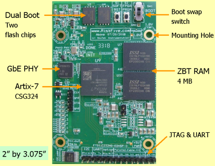
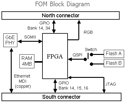
The FPGA On Module (FOM) is shown below. It is a small plugin board with the core hardware: the FPGA, the boot flash, the RAM memory, the gigabit Ethernet transceiver (PHY), and power. The FOM will be hosted by a motherboard providing other functions: the SD card, USB, video, and other connectors needed for a particular application. The FOM will be connected to a motherboard with two high-density Hirose connectors, secured with four mounting screws.


Major Features.


Technical specs.

  • FPGA specifications.
  • Number of pins: 324 on a 0.8 mm grid.
  • FPGA type: Artix-7 from 15T to 100T.

  • Video specifications.
  • VGA output with 24 bit color is generated by the Analog Devices chip ADV7125.
  • Monitor resolution is defined by driving the HSYNC and VSYNC video strobes.

  • Digital I/O specifications.
  • GPIO pins are available to the motherboard via the Hirose connectors.
  • All GPIO pins are connected to Artix High Range (HR) banks.
  • The voltage range of the HR pins can be up to 3.3V.
  • Most of these pins are arranged as differential pairs.
  • All digital I/Os are processed in the FPGA firmware.

  • Ethernet specifications.
  • The Gigabit Ethernet chip type DP83867CSRGZT is connected directly to the FPGA.

  • Memory specifications.
  • Two ZBT chips type IS61NLP102418B-200B3L are connected to the FPGA.
  • Memory capacity: 4 MB.
  • Memory interface width: 32 bits.
  • Memory clock speed: up to 200 MHz.
  • Nominal throughput: up to 800 MB/s.

  • Boot memory specifications.
  • Two SPI flash chips are connected to the FPGA with a quad SPI (QSPI) interface.
  • The flash chip capacity can be anywhere from 4 MB up to 32 MB.
  • We will populate the boards with either 16 MB or 32 MB flash chips, depending on availability when the boards are manufactured.
  • Either one of the chips can be used to boot the FPGA.
  • The user can select the boot flash A or B using a mechanical slide switch.
  • In case the dual boot is not needed, one chip can be used to boot, while the other can implement an embedded Solid State Disk.

  • JTAG.
  • The boot configuration file will be loaded to flash with a JTAG cable.
  • We recommend to use FTDI cable type C232HD-EDHSP-0 for JTAG.
  • A free utility named fpgaprog can be used with that cable.
  • Xilinx IMPACT can also be used with one of Xilinx programming cables.

  • UART.
  • UART pins Tx, Rx are provided on the same pin header.
  • UART pins CTS#, RTS# are provided, though these are rarely used.
  • The FTDI cable type C232HD-EDHSP-0 can be used for UART.
  • Other similar USB-to-UART cables can be used as well.

  • SPI and I2C.
  • SPI and I2C pins are pinned out to the motherboard.

  • Wireless.
  • The 8 - pin header on the motherboard is arranged according to the NRF24L01 pinout.
  • The NRF24L01 wireless module was used for the original 2013 FPGA Oberon project.
  • The same wireless module is also commonly used with Arduino.
  • The wireless networking with the NRF24L01 module is supported with both the Arduino and the original 2013 FPGA Oberon System.

  • Diagnostic LEDs.
  • Eight diagnostic LEDs are provided, driven by an I2C expander chip.
  • These LEDs are provided for displaying boot progress, status display, or other uses.

  • Power.
  • High current +5V power is provided by the motherboard, using one of the mounting holes.
  • The FTDI cable type C232HD-EDHSP-0 can power the FOM during development (up to 450 mA).
  • A standalone +5V power supply can also be used.
  • All the voltages needed by the FPGA are generated by the FOM board.
  • The FOM can output fixed +3.3V and +1.8V to power circuitry on the motherboard.
  • The FOM can generate 1.2V, 1.5V, 1.8V, 2.5V, or 3.3V for FPGA banks 15 and 16.
  • One of these voltages is selected with a DIP switch.

  • Firmware development specifications.
  • All the Artix-7 FPGAs are supported by the free Vivado WebPack from Xilinx.
  • The 100T chip is also supported under ISE WebPack from Xilinx.

  • Software and operating system specifications.
  • The board can run any operating system supported by one of many soft processor cores running in the Artix-7 gate array.

  • Open source.
  • The board schematics will be released as a PDF file when the boards are committed to manufacturing.
  • The FPGA configuration framework will be released in source to allow 3rd parties to develop their firmware.

Please inquire concerning other specs and details that have not been covered above.


Purchasing the RiskFive FPGA System.

The boards will be available for purchase soon. Please inquire by sending an e-mail from the contact page.


Updated Oct/13/2018.
© 2018 by SkuTek.com.